Research horizon
Additive manufacturing in semiconductor supply chains
A brief market watch on possible roles for complex ceramic and metal components in thermal management, tooling and equipment.
This KUNWU editorial note is based on the supplied technical source. Reported results belong to the described study or sample and are not KUNWU equipment specifications.
This paper is reproduced in the Public No. 3D Print Technology Reference, for the purpose of sharing information and resources, and is deleted.
How is 3D printing used in the high-end semiconductor industry? A message provides the answer.
In 2025, lithography giant ASML announced the establishment of the first qualified 3D printing supply chain for semiconductor parts.
This also means that 3D printing in the semiconductor industry is no longer a “show”. A detailed examination of the 3D printing process and the type of material currently available for use in the semiconductor industry can be described as diverse and will present examples in this period.
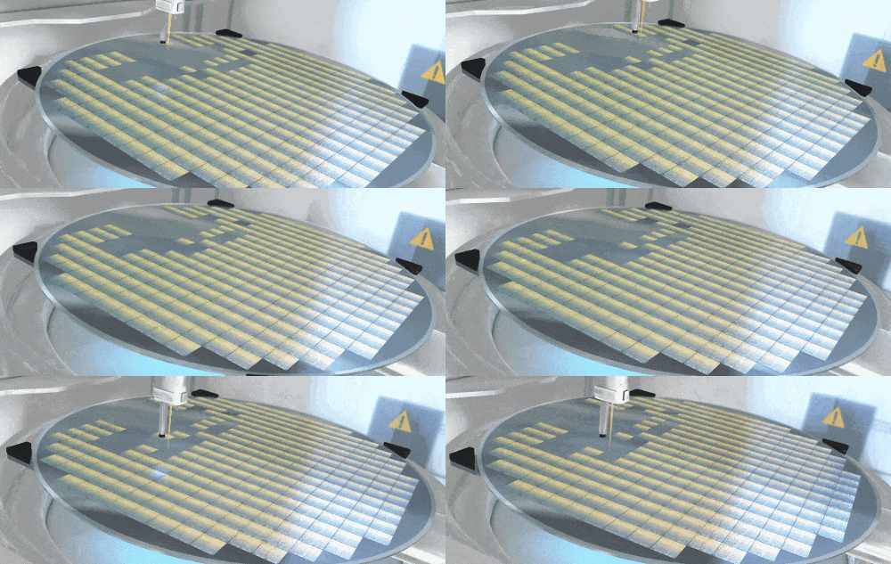
Production of cold spray coatings - Splash target
One of the key materials for the manufacture of semiconductor crystal circles is spatter target material, which is reported to have a direct impact on membrane mass by its purity, density and composition homogeneity.
The author's inquiry found that Chaozhuo Aviation stated in 2025 that it had used cold spray 3D printing technology to achieve target additive manufacturing, and had applied it in the semiconductor field, but the depth and breadth of application still need to be further expanded.
According to the report, the sputtering target manufactured by this technology has high purity, density, performance and deposition efficiency, the material is dense, almost defect-free, and has superior performance.
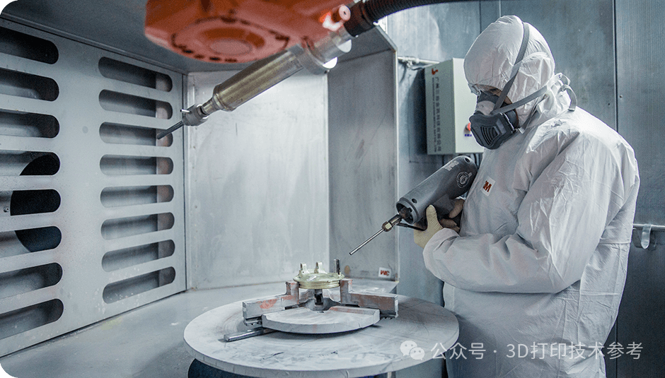
Ceramic 3D printing – semiconductor manufacturing equipment components
Another type of products that 3D printing participates in manufacturing are key components in semiconductor manufacturing equipment, such as wafer handling robot arms, electrostatic chucks, vacuum suction cups, etc., as well as internal materials in vapor deposition process chambers.
These components use technological ceramics such as ablution, aluminum oxide and silic oxide, which have high mechanical stability, electrical insulation and resistance to chemical corrosion, as well as heat stability.
Nowadays, 3D printing of these types of materials has reached the level of mass manufacturing, especially using ceramic 3D printing technology based on light curing.
The Austrian company Lithoz, which is well-known in the field of ceramic 3D printing, recently demonstrated a case about atomic layer deposition rings (ALD).
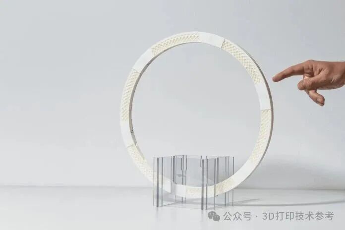
Lithoz Ceramic 3D Printed Atomic Layer Deposition Ring
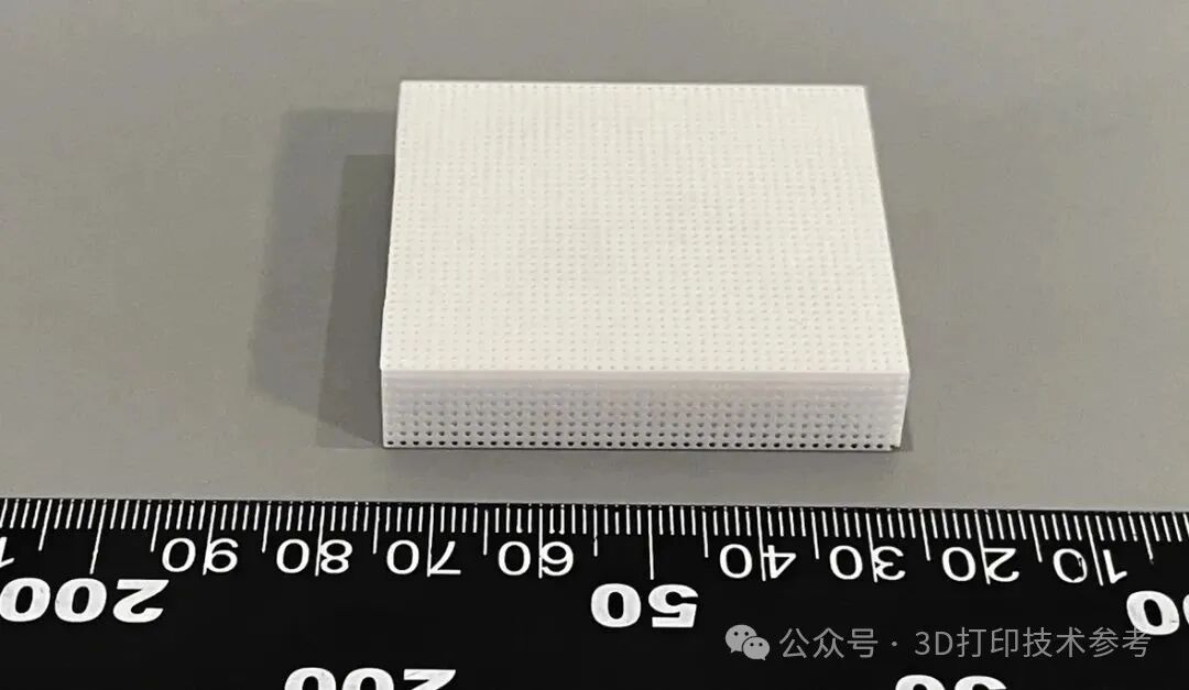
The LCM technology developed by Lithoz enables complex designs that were previously unachievable, with smooth surfaces targeting critical details and eliminating the need for connections and assembly. By integrating multiple functions into a single component and using additive manufacturing-based designs, not only can weight be reduced, but cost-effectiveness can also be increased. In addition, due to its stable process control, the LCM process enables reliable mass production.
Prodways offers two customized options for the semiconductor market, allowing manufacturers to optimize the production of delicate small parts and large complex parts without compromising performance or reliability.
Micro 3D printing technology - manufacturing ultra-high-precision probes
Probes in the semiconductor industry are core components that connect chips/wafers and test equipment for signal transmission, and play an important role in the quality control of semiconductor products.
Due to the small size of semiconductor products, especially the very small size of chip products, the size of the probe is required to reach the micron level. It is a high-end precision electronic component with high manufacturing technology content.

The author noticed that Exaddon, a Swiss company specializing in 3D printing of micro-metal parts, is manufacturing this high-precision part. It said that it is currently difficult to achieve pitches below 40µm in probe testing. Exaddon’s micro-3D printing technology overcomes these challenges. It is good at manufacturing independent structures with high aspect ratios and can manufacture high-quality metal parts with a size of less than 20µm.
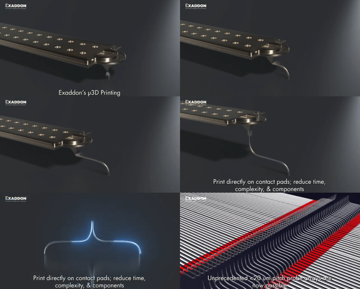
Exaddon micro-3D printing technology creates probes
The company demonstrated a MicroLED test array, using 3D printing technology to print directly on pre-patterned traces with a pitch of less than 20µm. The demonstration array has 128 probes with a minimum pitch of 18.5µm on the X-axis, 9.5µm on the Y-axis, and ±2µm on the Z-axis. Exaddon's probe array is approximately 10% the size of other companies' probe arrays, making MicroLED testers 64 times more efficient.
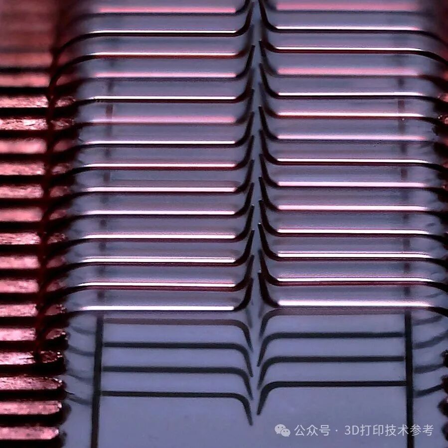
Optical microscopy image of the Exaddon128 probe array 3D printed directly on the contact pad
Laser 3D printing
High-precision manufacturing of semiconductor equipment components
The accuracy and reliability of semiconductor equipment directly affect the efficiency and yield of the semiconductor manufacturing process. Today, laser powder bed fusion 3D printing has the most applications in the semiconductor industry due to its advantages of high precision, integration and complex structure manufacturing. The comprehensive audit and qualification certification program developed by ASML for 3D printing suppliers is also targeted at this type of 3D printing process.
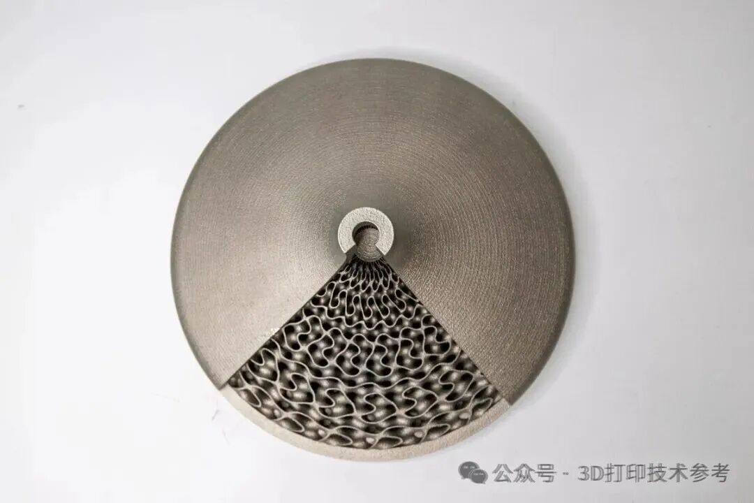
Wafer stages are critical components in semiconductor manufacturing, and by designing for additive manufacturing, internal cooling channels and surface structures can be optimized to significantly improve surface temperatures and thermal gradients while reducing time constants. With a unique design that can only be achieved through additive manufacturing, heat can be dissipated efficiently; structural optimization improves reliability, improves system throughput and accuracy, and improves overall performance.
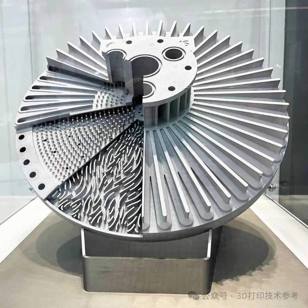
3D Systems 3D printed wafer stage thermal management components
3D Systems has launched a semiconductor wafer stage thermal management 3D printed part, highlighting the huge potential of this technology. It has a symmetrical radially arranged long strip structure that radiates outward from the center to form a shape similar to a fan blade. There are multiple lattice and fins of different sizes distributed on the surface. The overall design is precise and integrated manufacturing is achieved through 3D printing, which can be used for efficient heat dissipation.
Another application the company demonstrated was a showerhead used to uniformly deposit materials in semiconductor manufacturing. The pore structure and temperature stability of the nozzle are important factors that determine deposition uniformity. LPBF 3D printing technology enables control of the geometry of deposited non-cylindrical nozzles, more complex cooling channels for heat dissipation, and reinforced components to prevent leakage. Thousands of small holes are manufactured through 3D printing, with almost negligible impact on cost and production time.
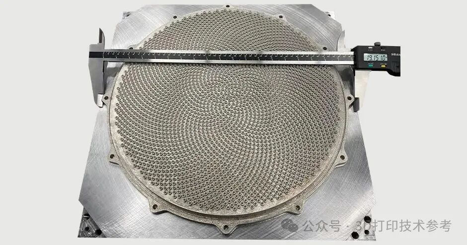
3D Systems 3D printing deposition nozzle
Critical components of semiconductor equipment require materials with excellent corrosion resistance without affecting performance or system uptime. The author noticed that EOS has launched a commercial pure nickel alloy NiCP with a minimum purity of 99.0%. The introduction of this material changes the way semiconductor manufacturers design and produce components, eliminating the traditional limitations of protective plating while increasing component life.
END
The application potential of additive manufacturing technology in the #semiconductor industry is huge, and its application scope and process types are believed to far exceed the examples and types listed in this article.
However, the quality of 3D printed parts is believed to have extremely high requirements in this industry. ASML's QAM team performed a failure mode assessment for a specific additive manufacturing process, requiring suppliers to refine risk definitions based on expert opinion. Its core goal is to reduce process variables that impact the repeatability of process output and set a benchmark for standardized additive manufacturing production in high-risk industries such as semiconductor manufacturing.