Applications
Electrical traces on three-dimensional ceramic surfaces
Combining printed ceramic, laser activation and electroless deposition enables conductive traces on three-dimensional parts.
This KUNWU editorial note is based on the supplied technical source. Reported results belong to the described study or sample and are not KUNWU equipment specifications.
Ceramic plates are excellent, but it has been an industry challenge to "crawl" on the 3D ceramic surface of the circuit. The South-East University team published an updated study in Advanced Materiels: combining 3D printing of DLP ceramics with selective chemical plating of laser activation, creating a low-cost, customized new path for 3D ceramics by "length" 60 micrometre wide copper circuits on 3D ceramic surfaces.
Good ceramics, difficult three-dimensional circuits
In aerospace, 5G/6G communications, radar and other fields, LTCC (low temperature co-fired ceramic) has always been the mainstream substrate for radio frequency microwave devices due to its high strength, high thermal stability and high frequency and low dielectric loss.
However, traditional LTCC manufacturing relies on the lamination process of "casting → drilling → silk screen → lamination → co-firing", which has two unavoidable limitations:
- Planar limitation: conventional lamination stacks two-dimensional layers and makes complex three-dimensional integration difficult.
- Batch-size limitation: major equipment and process investment and long production cycles make small-batch customization and rapid prototyping costly.
Ceramic 3D printing allows complex three-dimensional structures to be formed at one time, but printing the shape is only the first step. How to make high-precision metal circuits on the surface of 3D ceramics is the real sticking point: the conductivity of co-fired silver paste is low; deposition processes such as PVD and DPC rely on photolithography patterning, which is inherently only suitable for flat surfaces.
In response to this contradiction, the team of the Key Laboratory of MEMS of the Ministry of Education of Southeast University proposed a hybrid additive manufacturing (HAM) route: DLP ceramic 3D printing + laser activation selective electroless plating (LASELP). The results were published in the top journal "Advanced Materials" in materials science.
Printing, laser activation and electroless plating
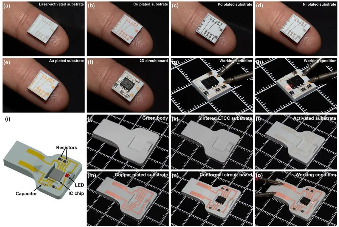
The entire process chain can be summarized into six steps (Figure 1):
- 1. Slurry: mix LTCC powder, ATO (antimony tin oxide) catalyst and photosensitive resin to produce a selectively plateable ceramic feedstock.
- 2. Printing: DLP photopolymerization forms the ceramic green body layer by layer.
- 3. Debinding and sintering: a 2 h dwell at 850 °C produces the dense ceramic substrate.
- 4. Activation: a 1064 nm near-infrared laser patterns the ceramic surface and converts Sn IV into catalytic Sn II plating seeds in the activated areas.
- 5. Plating: copper deposits selectively in activated regions; ENIG subsequently adds protective nickel and gold layers.
- 6. Assembly: solder the components to obtain the three-dimensional ceramic electronic device.
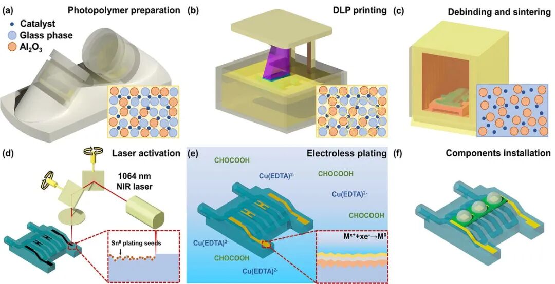
The clever thing about this route is that catalysts are pre-positioned into ceramics, and lasers are only responsible for "awakening" areas that need metalization -- no matter how complex the surface, the lines can grow.
A printable slurry that can be selectively metallized
To make "printing" and "platable" compatible, the slurry formula is the first difficulty. Ordinary laser-activated catalysts (such as Cu₂(OH)PO₄, PdCl₂, etc.) have low decomposition temperatures, and the high temperature of ceramic sintering will cause them to "deactivate" in advance; while heat-resistant catalysts such as CuCr₂O₄ will strongly absorb ultraviolet light, destroying the curing accuracy of DLP printing.
The team finally chose ATO (antimony tin oxide) as the catalyst and used TiO₂ to enhance the infrared absorption of the matrix. The proportion of ceramic raw materials in the formula was 96 wt% LTCC + 3 wt% ATO + 1 wt% TiO₂. This choice satisfies three hard constraints simultaneously:
- Thermal stability: XPS shows that ATO retains stable Sn IV after 850 °C sintering, preserving its potential for subsequent laser activation.
- Optical compatibility: ATO absorbs limited UV light, allowing suitable cure depth and printing accuracy.
- Printability: at 1.5 wt% dispersant, minimum viscosity is approximately 1500 mPa·s. Exposure of 180 mJ/cm² gives about 100 μm cure depth, suitable for 50 μm layers.
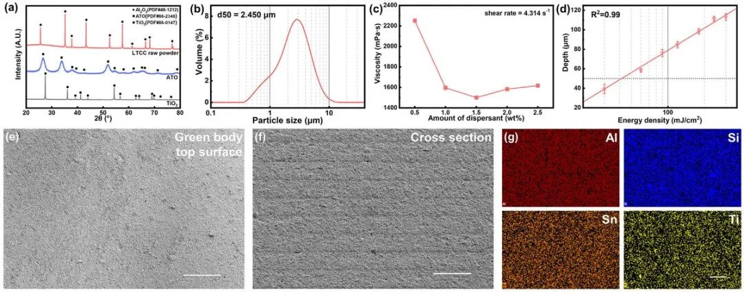
The green body was degreased at ultra-low speed and sintered at 850°C for 2 hours to obtain a blue-gray dense ceramic with a density of 3.25 g/cm³, a three-point bending strength of 302.3 MPa, and a dielectric loss of only 0.0133 at 25 GHz. Its comprehensive performance is comparable to commercial LTCC products.
How laser activation enables plating
There is only one key scientific question in the entire technology: What exactly does the laser do to the ceramic surface?
XPS analysis gave the answer: after sintering, the Sn element in ATO is stable in the SnIV state (binding energy 487.1 eV); and after 1064 nm laser irradiation, a new SnII characteristic peak (486.1 eV) appears in the activation zone - the laser reduces the stable SnIV in situ to catalytically active SnII, which is the classic "seed" for electroless copper plating.
The subsequent chemical plating is a "several reaction": copper ion is reduced to copper particles by the SnII seed, and copper particles are used as self-catalyzing points to sustain the plating and accumulate layers. The growth was clearly documented by SEM: three minutes of copper nanoparticles, 10 minutes of shining copper layers and 30 minutes of metallic cover.
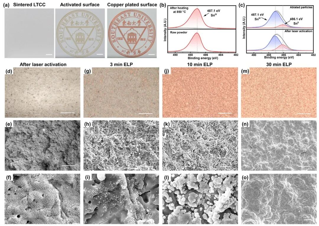
In Figure 3(a), laser-patterned regions forming the Southeast University emblem receive complete copper coverage while unactivated regions remain unplated. Within the tested parameter set, 8 W and 1000 mm/s gave the lowest line resistance. Insufficient power caused incomplete activation; excessive power ablated the surface.
60 μm lines and 88% of pure-copper conductivity
The quality of the process ultimately depends on data. The team’s systematic characterization results of the electroless copper plating layer are as follows:
| Property | Measured result | Note |
|---|---|---|
| Minimum line width | 60 μm | Minimum gap 70 μm; 28 interdigitated pairs without short circuits |
| Copper thickness | ~11 μm after 4 h plating | Meets the reported skin-depth requirement above 0.1 GHz |
| Conductivity | 5.1 × 10⁷ S/m | ~88% of pure copper |
| Copper purity | >99 wt% | No CuO/Cu₂O secondary phase detected by XRD |
| Adhesion | ASTM D3359 class 5B | No detachment in tape testing |
| Surface roughness | Sa 1.41 μm | Comparable to very-low-profile copper foil for high-frequency PCBs |
| ENIG thermal stability | Stable resistance after 2 h at 500 °C | Bare copper oxidized to an open circuit at 300 °C |
Table 1 · Summary of key performance indicators of LASELP copper layer
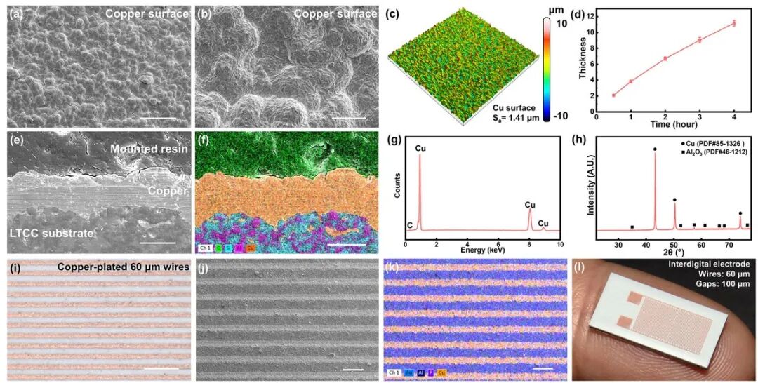
The 60μm line width is close to the mass production level of precision PCB, far better than the 100-200μm of co-fired silver paste, and is realized on 3D free-form surfaces. Surface roughness below 2 μm is particularly critical for high-frequency devices—rough surfaces will significantly increase microwave loss. This work directly benchmarks commercial high-frequency PCB copper foil.
In response to harsh conditions, the team further introduced the ENIG (Chemical nickel impregnation) process, which forms the Cu/Ni-P/Au three layers of composite plating: nickel to block proliferation, gold to ensure weldability and antioxidation. In the heat shock experiment, the ENIG sample was 500 °C at 2 hours of resistance stable, and the naked copper line was 300 °C.
Three demonstrations of ceramic electronics
Blinking circuits on flat and conformal substrates
The team produced an ENIG circuit with a line width of 150 μm on a ceramic substrate the size of a fingernail. After mounting the components, the LED flashed steadily at about 1.5 Hz. The same circuit was also "moved" onto a 3D conformal substrate with a 45° slope - this is a structure-function integrated design that cannot be achieved by planar technology.
Water cooling for a high-power LED
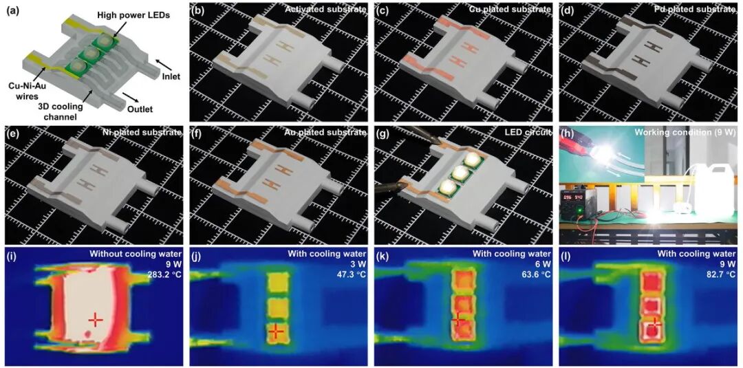
Thermal management is the lifeblood of high-power electronics. The team directly integrated a conformal water-cooling channel inside the LED ceramic substrate, and the infrared thermal image comparison is extremely impactful: when 9 W is used without cooling, the chip soars to 283.2°C and burns out in 15 seconds; after passing in 60 mL/min cooling water, the full power operation is only 82.7°C.
A directional three-dimensional UV sensor
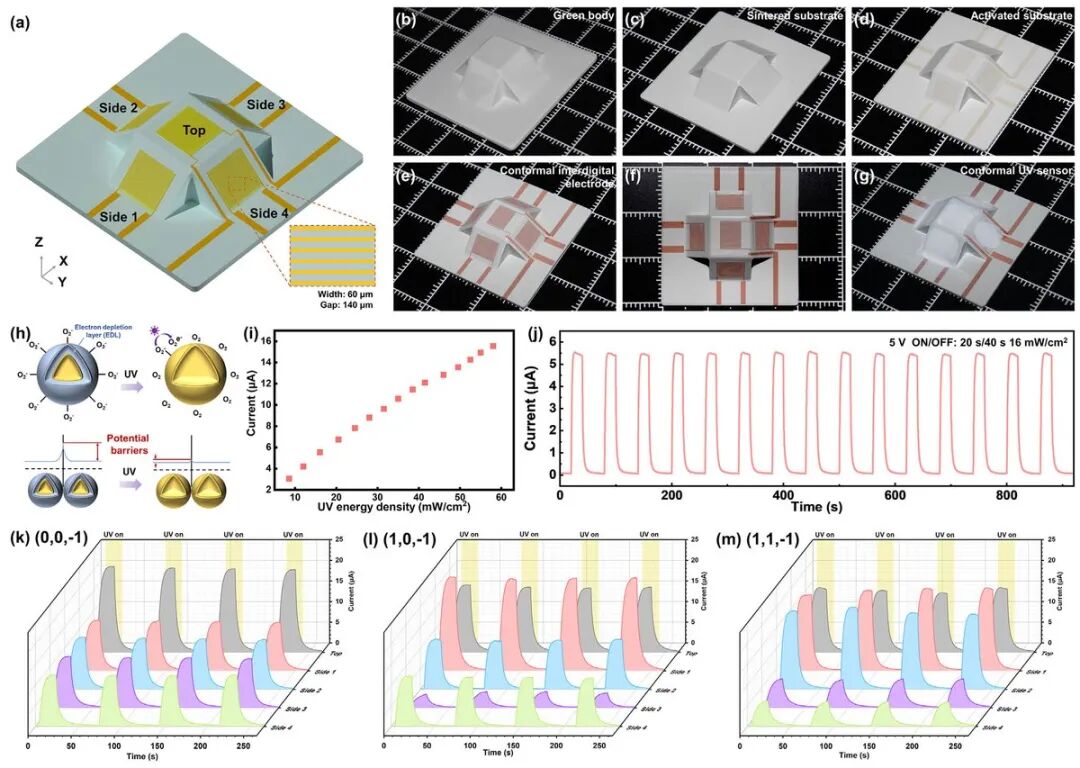
The most imaginative demonstration is a 3D UV sensor: five fork finger electrode units are placed on top of the base plate and four 45° slopes, with Zno dripping as a sensor. The electrodes are in different directions, with 22.4 μA and only 3.9 μA on the back side, and combined algorithms can reverse the 3D into the light vector - This is a function that the plane sensors can't do naturally.
Three implications for ceramic additive manufacturing
First, material design is the source of functional breakthroughs. The core is not new equipment, but the material ingenuity of "pre-embedding" the catalyst into the slurry - the balance between ATO's heat resistance and light transmittance directly determines the success or failure of the process. Breakthroughs in functional ceramics increasingly rely on "slurry formulation".
Second, hybrid manufacturing is the only way to deviceization. The hybrid paradigm of "printing + laser + chemical plating" proves that the imagination of ceramic 3D printing lies in combining with mature downstream processes, rather than replacing everything.
Third, 3D circuits allow ceramic electronics to return to "structure is function". Conformal cooling channels and directional sensing arrays directly convert structural freedom into device performance - this is the core value of ceramic 3D printing.
Reference papers: Wang P, Chen Li (Key Laboratory of MEMS, Ministry of Education, Southeast University)