Research horizon
Two-photon microstructures in glass, ceramic, metal and carbon
The review follows two-photon lithography from polymer templates to inorganic microstructures through different conversion routes.
This KUNWU editorial note is based on the supplied technical source. Reported results belong to the described study or sample and are not KUNWU equipment specifications.
A research team from Southeast University recently published a review in the international materials journal "Small", systematically sorting out the latest manufacturing progress of four types of inorganic materials: glass, ceramics, metals, and carbon under two-photon lithography (TPL). This laser direct writing technology can shape materials into three-dimensional microstructures with characteristic dimensions of only a hundred nanometers. This article will help you quickly see how to do this route, what it can do, and where it gets stuck.
A two-step route around incomplete conversion
Traditional ceramic 3D printing is first solidified into a green body and then degreased and sintered. The scale is usually in the millimeter range; while two-photon lithography directly targets sub-micron or even hundreds of nanometers. Its principle is not complicated: the femtosecond laser is focused into the interior of the photosensitive resin, using nonlinear two-photon absorption to trigger cross-linking only at the focus, thus writing out a three-dimensional skeleton point by point like "voxel-level engraving."
Here is a key premise that deserves to be clarified. Normal single photo fixation is "consolidation of the whole line of light" and accuracy is subject to optical fracturing limits; double photon absorption depends on light-high-square relationships. Only the small area with the highest light in the vicinity of the focus reaches the conjunctivity threshold, so solidification volumes are compressed to the "physical" scale of the sub-fault limit. This type of body matter, which is a rag, is able to collide complex three-dimensional features that are difficult to access even by traditional processes. This is also where the two photons can be transplanted to the bottom of the inorganic material after being carved in optical and microelectronics.
What really makes inorganic materials "come into play" is the subsequent heat treatment. What is printed first is not the final part, but a polymer or organic-inorganic hybrid "blank", which is then transformed into dense glass, ceramics, metal or carbon through pyrolysis, annealing or sintering. This two-step strategy of "print first, then convert" is the core framework throughout this review. Its advantage is that it avoids the almost impossible task of "direct nanoscale processing of high-melting point inorganics". Because the material still exists in the form of easy-to-form resin during the printing stage, the problem of whether it is burned thoroughly is cleverly postponed to the heat treatment stage.
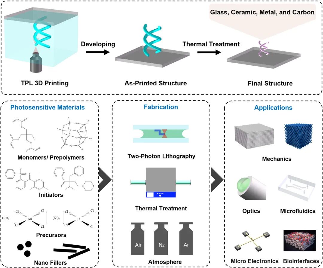
Four material classes and their inorganic-conversion recipes
The same principle of "print first, then convert" applies to different materials, but the design of the precursor and the heat treatment window are completely different. There is no way to combine these four categories and can only be dismantled one by one.
Glass is one of the most mature. Precursors represented by POSS (polyhedral oligomeric silsesquioxane) can achieve vitrification without destroying the microstructure by lowering the sintering temperature to about 650°C. The characteristic size can be within a hundred nanometers, providing a new molding method for photonic crystals and micro-optical components. The reason why POSS is popular is that it is an "organic cage with an inorganic core", has low shrinkage, high ceramic yield, and is more suitable than traditional siloxane for converting into a glass phase while maintaining the morphology.
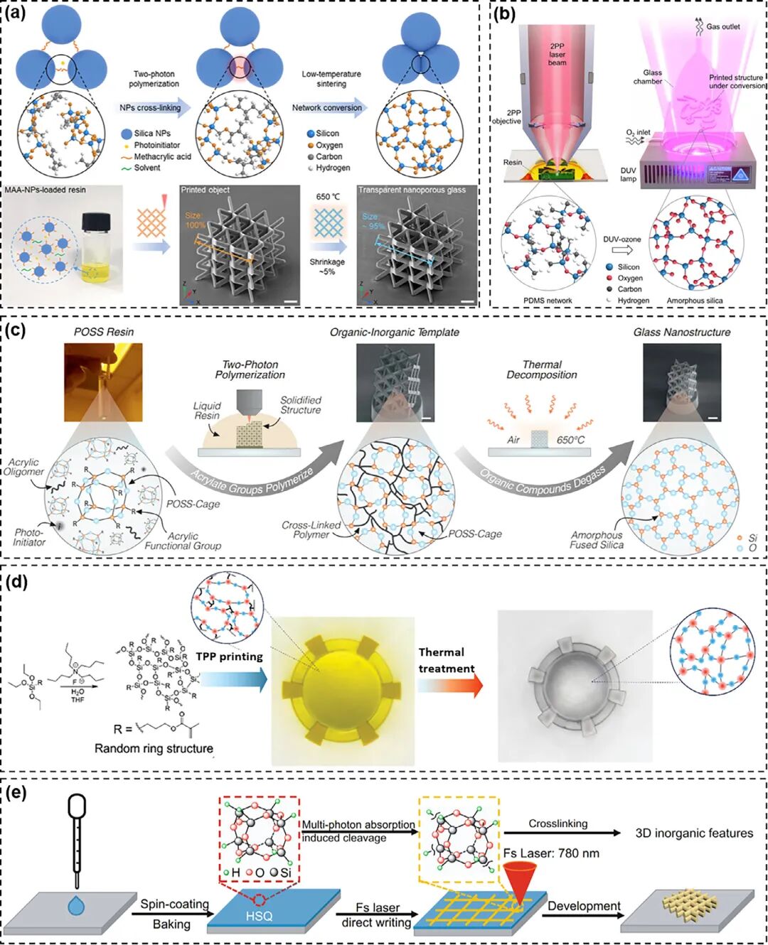
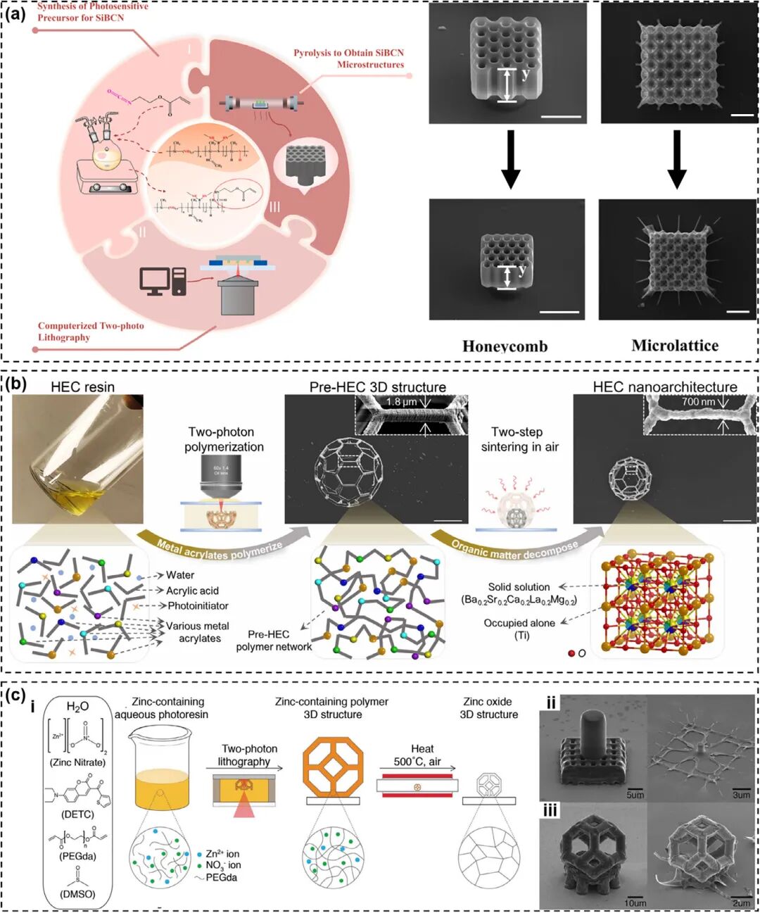
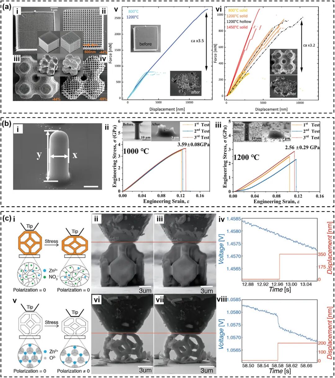
The porcelain strategy goes hand in hand with the glass, with a more diverse pre-pulse system and the best expression of the philosophy of "formulation determines fate". The polymer transformation ceramics (PDC) resin embeds elements such as Si, C, N, and B in a molecular chain, and thermally produces ceramics such as SiOC, SiCN, SiBCN, with a production rate of up to 76 wt per cent, characteristic size of 700 nm, resistant to pressure strength of 3.59 GPa. It's an elemental writing of ceramics into "polymers' skeletons," making transformation more uniform and more designable. Metal impregnation resins follow another path: they load metal salt into the resin, they are burned and provided with fine ceramics, with a maximum resolution capacity of 150 nm, which is also long in high resolution and functionality and integrates advanced responses such as voltage. The nanoparticle base resin (NPR), which consists directly of a highly solid nanopowder matrix, is the most recent of the four categories of "traditional pottery increments", which are the same source as the plasma logic printed by ceramic DLP.
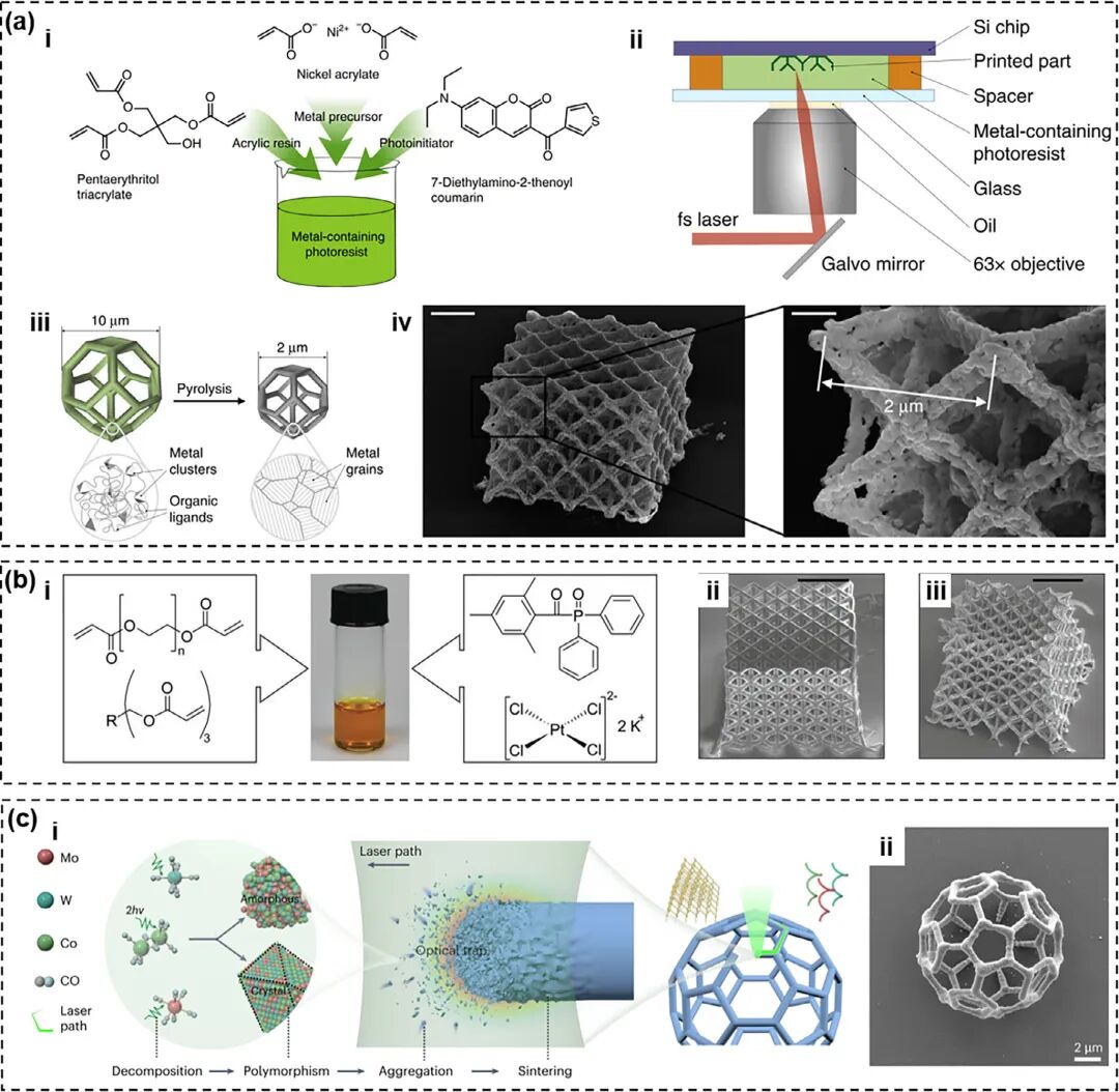
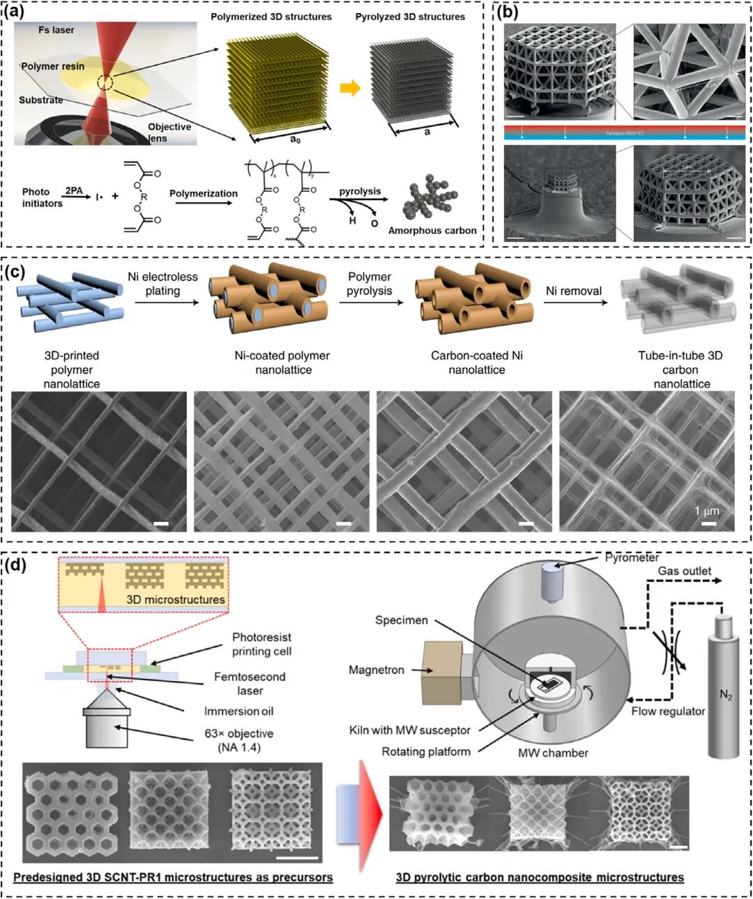
Metal and carbon show a greater "contrast". The two routes of metals are divided according to whether they have undergone chemical reduction: the non-reducing precursor physically embeds metal salts such as platinum and nickel or organic metal compounds into the resin. After printing, the metal is precipitated in situ from the polymer skeleton through high-temperature pyrolysis and reducing atmosphere. The characteristic size of the nickel nanocrystal lattice is therefore as low as 25-100 nanometers, and the specific strength reaches 2.1-7.2 MPa·g⁻¹·cm³, is the leader in strength and density at this scale; the platinum microstructure has higher purity, and the electrical conductivity is close to 67% of the bulk material. Another reduction precursor route uses gold and silver ions as objects and relies on in-situ photochemical reduction by laser during printing. It does not require high-temperature pyrolysis and only requires low-temperature annealing. It is more suitable for high-speed direct writing of precious metal microstructures. Carbon takes a different approach, relying on high-yield carbonization of resins. The pyrolyzed glassy carbon nanolattice has a pillar diameter of only 200 nanometers, but its strength is close to 3 GPa, almost touching the upper limit of the theoretical strength of glassy carbon, while its density is only a fraction of that of bulk materials.
It can be said that the four routes are all "printing + heat treatment" on the surface, but the chemistry inside is completely different: glass focuses on low-temperature controllability, ceramics focuses on element conversion and yield, metal focuses on reduction mechanism and purity, and carbon focuses on carbonization yield and lightness. Read each one separately, and together it is a complete "inorganic microstructure process pedigree."
Performance changes at the micro- and nanoscale
These microstructures are really moving, and they're "small sizes" that make a leap in performance. In the case of ceramics, TPL prints the sintered YSZ nanostructure with a resolution of 500 nm and a pressure resistance of 4.5 GPa, which has been even higher than the block YSZ (2.0-3.8 GPa). When the size of the structure shrinks to the nanoscale, the material is closer to its theoretical strength limit. Behind this is the classic "smaller and stronger" effect: the limited scale of the defects, the finening of the crystals and the increase in the surface area, bringing the microcolumn closer to its theoretical carrying capacity under compression, in stark contrast to the normal pattern of large-scale ceramics, "vulnerable to defects and of strength far below theoretical values".
The emergence of functionality is equally amazing: the calcined ZnO nanolattice produces a voltage drop of 0.52 mV when compressed, "awakening" the piezoelectric effect, which means that functional ceramics no longer have to be limited to large-scale sintering, and the micro-nano structure itself can carry out sensing and energy conversion tasks; the "tube-in-tube" carbon structure obtained by catalytic carbonization of nickel has a density as low as 6.4 mg·cm⁻³, but it can achieve 30-50% large deformation recovery and excellent damping, and it can hold the two usually mutually exclusive properties of "ultra-light" and "strong" at the same time. Multiple transitions in density, strength, electricity, and mechanics are all realized simultaneously on the micro-nano scale.
Three remaining barriers
Although the prospects are attractive, there are still three hurdles ahead for the creation of inorganic microstructures by two-photon lithography, each of which is directly aimed at mass production.
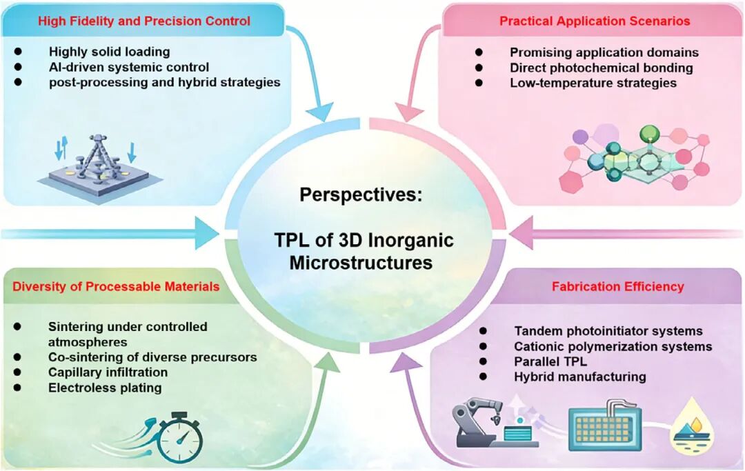
One is constriction and cracking: solid content is difficult to achieve — low-condensed resin tends to produce significant volume contractions in thermally decompressed sinters, and internal stress and organic composition escapes easily leading to microfracking and destruction of sub-mibular skeletons; and an increase in the adhesive content tends to trigger separation and reunification with nanoparticles, but instead increases bodyin and reduces resolution. There's not a single single generic formula between size and printability. The second is throughput: it is slow by the very nature of a single point-by-point writing, which is the price it has to pay for its "precision crushing"; although parallel programmes such as space-based photomodifiers and distilling optical components have increased the bodyinity rate to 108 quantities, it is still a water truck for projects that require hundreds of millimeters, with a volume gap from industrial capacity. The third is material diversity: high-performance inorganic systems such as nitrogen oxides (Si3N4, AlN), which are still difficult to stabilize because of the hard conditions of pre-pulsive synthesis and thermal transformation. Glass, ceramics, metals and carbon are rich, but they also represent only a fraction of the inorganic material.
Micro/nanofabrication and scale-up serve different needs
Putting the three hurdles together, you can understand the positioning of two-photon lithography: it is not to replace the existing ceramic 3D printing, but to fill in the "submicron to nanometer" scale range that has long been left blank by traditional processes. Micro-optical devices, photonic crystals, micro-electromechanical systems, and ultra-light metamaterials are the arena where it can best demonstrate its capabilities. For the mass production of millimeter-level precision ceramic structural parts, mature routes such as DLP and direct writing are still more pragmatic choices. "Writing" step by step and "laying" layer by layer are essentially two different industrial logics.
The two routes, one micro and one macro, complement each other and together support the complete landscape of inorganic additive manufacturing from nanometers to millimeters. For scientific research and industrial users who are concerned about precision ceramic molding, to see this map clearly, they must not only know "what new possibilities are there at the nanoscale", but also keep in mind "who is the most reliable choice for mass production at the millimeter scale", and distinguish their respective divisions of labor, so that they can choose the right path for specific projects.
Reference papers
Liu X, Li Y, Huang Y, et al. Recent Advances in Two-Photon Lithography of 3D Inorganic Microstructures: Glass, Ceramics, Metals, and Carbon. Small, 2026. DOI: 10.1002/smll.74770